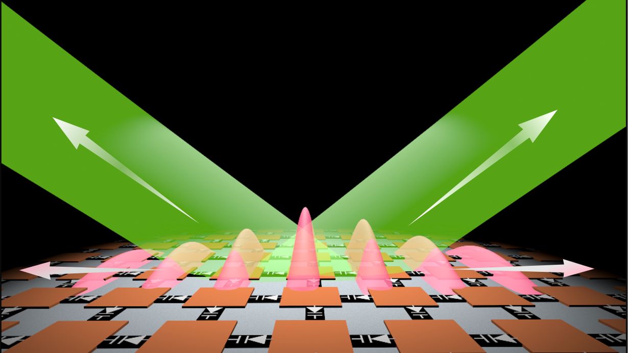
Photonic time crystals, whose properties change periodically, promise significant enhancements in microwave engineering, optics, and photonics. Researchers from Karlsruhe Institute of Technology (KIT) and partners from Aalto University and Stanford University have unveiled a groundbreaking 2D photonic time crystal and demonstrated important applications. Their approach simplifies the realisation of photonic time crystals and may improve the efficiency of future communication systems. The results of this study have been reported in Science Advances. (DOI: 10.1126/sciadv.adg7541)
In the broadest sense, time crystals belong to the so-called metamaterials, which are artificially produced materials that exhibit properties that do not occur in nature. The fascinating concept of time crystals was first introduced by physics Nobel Prize Laureate Frank Wilczek in 2012. Unlike ordinary crystals, time crystals do not change their properties in space, but periodically in time. Researchers in photonics are currently working on the first optical versions of these materials, called photonic time crystals. These crystals have shown great potential in enhancing wireless communication signals and the new generation of laser systems, as electromagnetic waves traveling in photonic time crystals can be amplified effectively.
Dimension Reduction Facilitates the Implementation
However, research on photonic time crystals has so far focused on bulk materials – that is, three-dimensional structures. Implementing bulk photonic time crystals has proven to be enormously challenging, and the experiments have not yet gone beyond model systems with no practical applications. Researchers from the Institute of Nanotechnology (INT) and the Institute for Theoretical Solid State-Physics (TFP) of KIT, together with partners from Aalto University in Finland and Stanford University in the USA, have now developed a new approach and presented the results in the Science Advances journal: The team succeeded in creating the first two-dimensional photonic time crystal ever. This is actually a very thin layer of such a metamaterial. “We found that reducing the dimensionality from a 3D to a 2D structure made the implementation much easier, which made it possible to realize photonic time crystals,” explains Dr. Xuchen Wang, the lead author of the study, who is currently conducting research at KIT in the group lead by Professor Carsten Rockstuhl. The team designed and synthesized a two-dimensional electromagnetic structure with embedded tunable components periodically to dynamically repeat its electromagnetic property in time. With the 2D structure, they experimentally verified the theoretical predictions about its behavior. “Based on this discovery, we observed, for the first time, strong wave amplification in photonic time crystals,” says Wang.
2D Photonic Time Crystals for More Efficient Communication
This breakthrough discovery can lead to significant advancements in various technologies, such as wireless communication, integrated circuits, and lasers. By amplifying electromagnetic waves, it will be possible to build more powerful and efficient wireless transmitters and receivers in the future. What is more, coating surfaces with 2D photonic time crystals could also reduce signal decays in wireless transmission, a bottleneck problem in wireless transmission. 2D photonic time crystals could also simplify laser design, avoiding the need for complex bulk mirrors typically used in lasing cavities.
Another critical application emerges from the finding that 2D photonic time crystals don’t just amplify the incoming electromagnetic waves in free space but also waves traveling along the surface. Surface waves are used for communication between electronic components in integrated circuits. “When a surface wave propagates, it suffers from material losses, and the signal strength is reduced. With 2D photonic time crystals covering the propagation media, the surface wave can be amplified, and communication efficiency enhanced,” says Wang.
Original publication
Xuchen Wang, Mohammad Sajjad Mirmoosa, Viktar S. Asadchy, Carsten Rockstuhl, Shanhui Fan, & Sergei A. Tretyakov: Metasurface-Based Realization of Photonic Time Crystals. Science Advances, 2023. DOI: 10.1126/sciadv.adg7541
https://www.science.org/doi/10.1126/sciadv.adg7541
More about KIT Materials Center

