
Ultrafast, efficient, and reliable single-photon detectors are among the most sought-after components in photonics and quantum communication, which have not yet reached maturity for practical application. Physicist Dr. Wolfram Pernice of the Karlsruhe Institute of Technology (KIT), in cooperation with colleagues at Yale University, Boston University, and Moscow State Pedagogical University, achieved the decisive breakthrough by integrating single-photon detectors with nanophotonic chips. The detector combines near-unity detection efficiency with high timing resolution and has a very low error rate. The results have been published by Nature Communications (doi:10.1038/ncomms2307).
Without reliable detection of single photons, it is impossible to make real use of the latest advances in optical data transmission or quantum computation; it is like having no analog-digital converter in a conventional computer to determine whether the applied voltage stands for 0 or 1. Although a number of different single-photon detector models have been developed over the past few years, thus far, none have provided satisfactory performance.
Several new ideas and advanced developments went into the prototype developed within the “Integrated Quantum Photonics” project at the DFG Center of Functional Nanostructures (CFN). The new single-photon detector, tested in the telecommunications wavelength range, achieves a previously unattained detection efficiency of 91%.
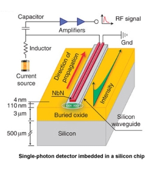
The detector was realized by fabricating superconducting nanowires directly on top of a nanophotonic waveguide. This geometry can be compared to a tube that conducts light, around which a wire in a superconducting state is wound and, as such, has no electric resistivity. The nanometer-sized wire made of niobium nitride absorbs photons that propagate along the waveguide. When a photon is absorbed, superconductivity is lost, which is detected as an electric signal. The longer the tube, the higher is the detection probability. The lengths involved are in the micrometer range.
A special feature of the detector is its direct installation on the chip, which allows for it to be replicated at random. The single-photon detectors built thus far were stand-alone units, which were connected to chips with optical fibers. Arrangements of that type suffer from photons being lost in the fiber connection or being absorbed in other ways. These loss channels do not exist in the detector that is now fully embedded in a silicon photonic circuit. In addition to high detection efficiency, this gives rise to a remarkably low dark count rate. Dark counts arise when a photon is detected erroneously: for instance, because of a spontaneous emission, an alpha particle, or a spurious field. The new design also provides ultrashort timing jitter of 18 picoseconds, which is 18 times 10-12 seconds.
The novel solution also makes it possible to integrate several hundreds of these detectors on a single chip. This is a basic precondition for future use in optical quantum computers.
The detector demonstrated in this study was designed to work at wavelengths in the Telekom bandwidth. The same detector architecture can also be used for wavelengths in the range of visible light. This would allow the principle to be employed in analyses of all structures that emit little light, i.e., photons, such as single molecules or bacteria.
C.V. Dr. Wolfram Pernice
Dr. Wolfram Pernice studied Microsystems Technology at Albert Ludwig University in Freiburg. After winning a research grant of the British Engineering and Physical Sciences Research Council he obtained his Ph.D. at the University of Oxford, England where he explored the Development of Efficient Numerical Methods for Simulating Photonic Devices. In 2008 he joined Yale University where, supported by a Humboldt scholarship, he analyzed nano-opto-mechanical systems in the group of Hong Tang. In summer 2011, the German Research Association (DFG) appointed him as head of an Emmy Noether Research Group. His research into integrated quantum optical and nano-opto-mechanical systems had convinced the committee, and as the recipient of an Emmy Noether grant, he chose to pursue his work at the Karlsruhe Institute of Technology (KIT). Since October 2011, he has worked here as a Junior Group Leader at the Institute of Nanotechnology (INT). At the beginning of the year, he also won a Helmholtz International Research Group grant, which he wants to use to fund another post-graduate student in his Karlsruhe team.
The DFG Center of Functional Nanostructures (CFN) devotes its attention to the important area of nanotechnology and functional nanostructures. Its objective is to carry out excellent interdisciplinary and international research in order to produce nanostructures with new technical functions and take the first step from fundamental research to application. At the present time, more than 250 scientists and engineers cooperate in more than 80 sub-projects networked through the CFN in Karlsruhe, focusing on the areas of nano-photonics, nano-electronics, molecular nanostructures, nano-biology, and nano-energy. www.cfn.kit.edu
In close partnership with society, KIT develops solutions for urgent challenges – from climate change, energy transition and sustainable use of natural resources to artificial intelligence, sovereignty and an aging population. As The University in the Helmholtz Association, KIT unites scientific excellence from insight to application-driven research under one roof – and is thus in a unique position to drive this transformation. As a University of Excellence, KIT offers its more than 10,000 employees and 22,800 students outstanding opportunities to shape a sustainable and resilient future. KIT – Science for Impact.