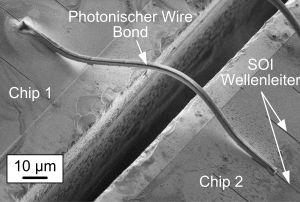
A team of KIT researchers directed by Professor Christian Koos has succeeded in developing a novel optical connection between semiconductor chips. “Photonic wire bonding” reaches data transmission rates in the range of several terabits per second and is suited perfectly for production on the industrial scale. In the future, this technology may be used in high-performance emitter-receiver systems for optical data transmission and, thus, contribute to reducing energy consumption of the internet. The scientists published their results in the journal “Optics Express“.
Communication processes can be made quicker and more energy-efficient with photonic components. Development of high-performance optical emitters and receivers integrated on microchips has already reached a high level. However, there have not yet been any satisfactory possibilities of bridging semiconductor chips optically. “The biggest difficulty consists in aligning the chips precisely such that the waveguides meet,“ explains Christian Koos, professor at the KIT Institutes of Photonics and Quantum Electronics (IPQ) and of Microstructure Technology (IMT) as well as member of the Center for Functional Nanostructures (CFN).
The team under Christian Koos tackles this problem from the other side: The researchers first fix the chips and then structure a polymer-based optical waveguide in a perfectly fitting manner. To adapt the interconnection to the position and orientation of the chip, the scientists developed a method for the three-dimensional structuring of an optical waveguide. They used so-called two-photon polymerization which reaches a high resolution. A femtosecond laser writes the free-form waveguide structure directly into a polymer that is located on the surface of the chip. For this purpose, the KIT researchers use a laser lithography system made by the Nanoscribe company, a spinoff of KIT.
Prototypes of the photonic wire bonds reached very small losses and a very high transmission bandwidth in the range of infrared telecommunication wavelengths around 1.55 micrometers. In first experiments, the researchers already demonstrated data transmission rates in excess of 5 terabits per second. Potential applications of photonic wire bonds lie in complex emitter-receiver systems for optical telecommunication as well as in sensor and measurement technology. As the highly precise orientation of the chips in manufacturing is no longer required, the process is particularly suited for the automatic production of large series. KIT researchers now plan to transfer this technology to industrial application in cooperation with partner companies.
N. Lindenmann, G. Balthasar, D. Hillerkuss, R. Schmogrow, M. Jordan, J. Leuthold, W. Freude, and C. Koos: Photonic wire bonding: a novel concept for chip-scale interconnects. Optics Express, Vol. 20, No. 16; 30 July 2012.
In close partnership with society, KIT develops solutions for urgent challenges – from climate change, energy transition and sustainable use of natural resources to artificial intelligence, sovereignty and an aging population. As The University in the Helmholtz Association, KIT unites scientific excellence from insight to application-driven research under one roof – and is thus in a unique position to drive this transformation. As a University of Excellence, KIT offers its more than 10,000 employees and 22,800 students outstanding opportunities to shape a sustainable and resilient future. KIT – Science for Impact.

