
Sunlight reflected by solar cells is lost as unused energy. The wings of the butterfly Pachliopta aristolochiae are drilled by nanostructures (nanoholes) that help absorbing light over a wide spectrum far better than smooth surfaces. Researchers of Karlsruhe Institute of Technology (KIT) have now succeeded in transferring these nanostructures to solar cells and, thus, enhancing their light absorption rate by up to 200 percent. The scientists report their results in the journal Science Advances. DOI: 10.1126/sciadv.1700232.
“The butterfly studied by us is very dark black. This signifies that it perfectly absorbs sunlight for optimum heat management. Even more fascinating than its appearance are the mechanisms that help reaching the high absorption. The optimization potential when transferring these structures to photovoltaics (PV) systems was found to be much higher than expected,” says Dr. Hendrik Hölscher of KIT’s Institute of Microstructure Technology (IMT).
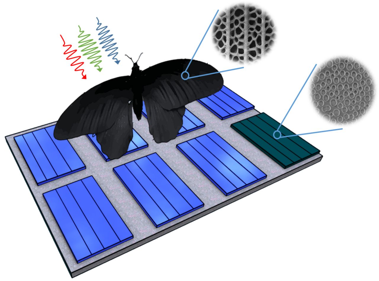
[Textfeld: Cross-connections between the ridges on the butterfly wing of Pachliopta aristolochiae form disordered “nanoholes” that enhance light absorption. (Photo: Radwanul H. Siddique, KIT/Caltech) Bio-inspired nanoholes etched into an amorphous silicon based photovoltaic absorber have a mean diameter of 238 nm. (Photo: Guillaume Gomard, KIT)] The scientists of the team of Hendrik Hölscher and Radwanul H. Siddique (formerly KIT, now Caltech) reproduced the butterfly’s nanostructures in the silicon absorbing layer of a thin-film solar cell. Subsequent analysis of light absorption yielded promising results: Compared to a smooth surface, the absorption rate of perpendicular incident light increases by 97% and rises continuously until it reaches 207% at an angle of incidence of 50 degrees. “This is particularly interesting under European conditions. Frequently, we have diffuse light that hardly falls on solar cells at a vertical angle,” Hendrik Hölscher says.
However, this does not automatically imply that efficiency of the complete PV system is enhanced by the same factor, says Guillaume Gomard of IMT. “Also other components play a role. Hence, the 200 percent are to be considered a theoretical limit for efficiency enhancement.”
Prior to transferring the nanostructures to solar cells, the researchers determined the diameter and arrangement of the nanoholes on the wing of the butterfly by means of scanning electron microscopy. Then, they analyzed the rates of light absorption for various hole patterns in a computer simulation. They found that disordered holes of varying diameters, such as those found in the black butterfly, produced most stable absorption rates over the complete spectrum at variable angles of incidence, with respect to periodically arranged monosized nanoholes. Hence, the researchers introduced disorderly positioned holes in a thin-film PV absorber, with diameters varying from 133 to 343 nanometers.
The scientists demonstrated that light yield can be enhanced considerably by removing material. In the project, they worked with hydrogenated amorphous silicon. According to the researchers, however, any type of thin-film PV technology can be improved with such nanostructures, also on the industrial scale.
Background information:
Thin-film PV modules represent an economically attractive alternative to conventional crystalline silicon solar cells, as the light-absorbing layer is thinner by a factor of up to 1000 and, hence, material consumption is reduced. Still, absorption rates of thin layers are below those of crystalline silicon cells. Hence, they are used in systems needing little power, such as pocket calculators or watches. Enhanced absorption would make thin-film cells much more attractive for larger applications, such as photovoltaics systems on roofs.
In close partnership with society, KIT develops solutions for urgent challenges – from climate change, energy transition and sustainable use of natural resources to artificial intelligence, sovereignty and an aging population. As The University in the Helmholtz Association, KIT unites scientific excellence from insight to application-driven research under one roof – and is thus in a unique position to drive this transformation. As a University of Excellence, KIT offers its more than 10,000 employees and 22,800 students outstanding opportunities to shape a sustainable and resilient future. KIT – Science for Impact.