
Scientists of Karlsruhe Institute of Technology (KIT) have succeeded in monitoring the growth of minute gallium arsenide wires. Their findings do not only provide for a better understanding of growth, they also enable approaches to customizing
nanowires with special properties for certain applications in the future. Gallium arsenide is a semiconductor material widely used in infrared remote controls, high-frequency technology for mobile phones, conversion of electric signals into light in glass-fiber cables, and solar cells for space technology. The results were presented in the journal “Nano Letters” by the team of Philipp Schroth of KIT and the University of Siegen.
For wire production, the scientists used the self-catalyzed vapor-
liquid-solid process (VLS process). Minute liquid gallium droplets are deposited on a hot silicon crystal of around 600°C in temperature. Then, this wafer is subjected to directed beams of gallium atoms and arsenic molecules that dissolve in the gallium droplets. After some time, nanowires start to grow below the droplets that act as catalysts for the longitudinal growth of the wires. “This process is quite well established, but it has been impossible so far to specifically control it. To achieve this, the details of growth have to be understood first,” co-author Ludwig Feigl of KIT says.
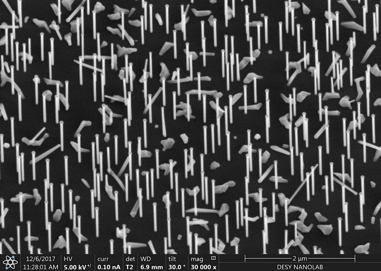
For the studies, the team used a portable chamber specifically designed by KIT’s Institute for Photon Science and Synchrotron Radiation (IPS) with funds of the Federal Ministry of Education and Research (BMBF). The researchers installed the chamber in the research light source PETRA III of the German Electron Synchrotron (DESY) and took X-ray pictures every minute to determine the structure and diameter of the growing nanowires. Finally, they measured the fully grown nanowires with an electron microscope. “We found that growth of nanowires is not only caused by the VLS process, but also by a second component that was observed and quantified directly for the first time in this experiment. This so-called side-wall growth makes the wires gain width,” says Philipp Schroth. In the course of the growth process, the gallium droplets become larger due to constant gallium vapor deposition. This has a far-reaching impact. “As the droplet size changes, the contact angle between the droplet and the surface of the wires changes as well. In certain cases, this causes the wire to suddenly continue growing with another crystal structure,” Feigl says. This change is of relevance to applications, as the structure and shape of the nanowires considerably affect the properties of the resulting material.
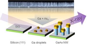
nanowires grow on a silicon wafer after bombardment of gallium droplets with gallium and arsenic. Growth can be monitored with the help of X-rays. The fully grown nanowires were examined by electron microscopy (background). (Figure: Philipp Schroth, KIT)
Original Publication in Nano Letters:
Radial Growth of Self-Catalyzed GaAs Nanowires and the Evolution of the Liquid Ga-Droplet Studied by Time-Resolved in situ X‐ray Diffraction; Philipp Schroth, Julian Jakob, Ludwig Feigl, Seyed Mohammad Mostafavi Kashani, Jonas Vogel, Jörg Strempfer, Thomas F. Keller, Ullrich Pietsch, and Tilo Baumbach; „Nano Letters“, 2018; DOI: 10.1021/acs.nanolett.7b03486
Additional material:
Publication in “Nano Letters“: https://pubs.acs.org/doi/10.1021/acs.nanolett.7b03486
Being “The Research University in the Helmholtz Association”, KIT creates and imparts knowledge for the society and the environment. It is the objective to make significant contributions to the global challenges in the fields of energy, mobility, and information. For this, about 10,000 employees cooperate in a broad range of disciplines in natural sciences, engineering sciences, economics, and the humanities and social sciences. KIT prepares its 22,800 students for responsible tasks in society, industry, and science by offering research-based study programs. Innovation efforts at KIT build a bridge between important scientific findings and their application for the benefit of society, economic prosperity, and the preservation of our natural basis of life. KIT is one of the German universities of excellence.