
Karlsruhe Institute of Technology (KIT) and ETH Zurich plan to conduct joint research into new types of integrated circuits for communications networks, which are characterized by their atomic dimension and their energy efficiency. To this end, the Swiss Werner Siemens-Foundation has donated CHF 12 million (approx. EUR 10.5 million) for the establishment of the joint Centre for Single-Atom Electronics and Photonics.
“I would like to thank the Werner Siemens-Foundation for enabling KIT and ETH Zurich to complement each other’s expertise within this cross-border cooperation, which I am certain will be of benefit to research, teaching, and innovation on both sides,” says Professor Holger Hanselka, President of KIT.
“The generous donation from the Werner Siemens-Foundation provides a unique opportunity to pool the skills of KIT and ETH in the field of electronics and photonics of individual electrons. This will strengthen fundamental research and accelerate the translation into practical applications,” says ETH President Lino Guzzella.
“We hope our donation will lead to a major breakthrough in the area of communications technology,” says Dr. Hubert Keiber, Chair of Trustees of the Werner Siemens-Foundation. According to Keiber, the research to be conducted at the Centre for Single-Atom Electronics and Photonics will be revolutionary, making it a good match for the Foundation’s portfolio.
The volume of data transmitted and processed via communications networks around the globe is growing steadily. This also means that all network components have to become more efficient. These components include so-called modulators that convert the information initially available in electronic form into optical signals. Thousands of such modulators are used in computing centers. As every modulator still is several centimeters long, much space is required.
For this reason, researchers of KIT and ETH Zurich intend to develop and study new types of integrated circuits with components that operate at the level of individual atoms and are therefore miniscule in size, but can still be integrated into existing industrial CMOS technology. To this end, they are now establishing the Centre for Single-Atom Electronics and Photonics.
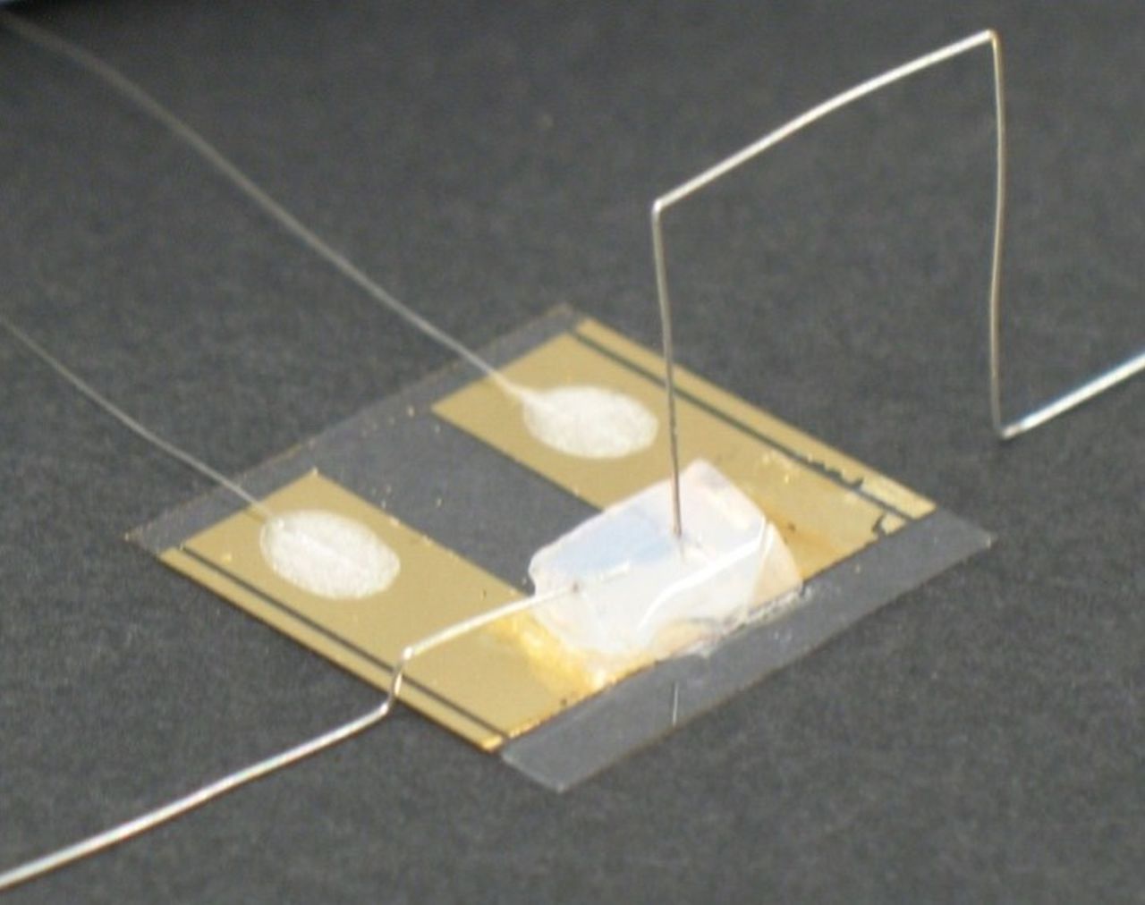
“At the new Centre, we plan to pursue an innovative research approach that is based on our latest findings which show that components with atomic dimensions not only work reliably, but are also more energy-efficient,” says coordinator Professor Jürg Leuthold of the Institute of Electromagnetic Fields of ETH. “With this new Centre, we now have a tool to translate fundamental research into single-atom switching devices into industrial prototypes and marketable products,” comments Professor Thomas Schimmel of KIT’s Institute of Applied Physics, who developed the first single-atom transistor worldwide in 2004. It consists of two electrodes that are separated by a single silver atom only. The position of the atom and, hence, conductivity between the electrodes is controlled by the voltage of the third, so-called gate, electrode. Due to the size and the materials used, this technology promises to give rise to highly energy-efficient, high-frequency switching devices that can be produced without any toxic substances.
In the next step, the researchers of KIT and ETH Zurich will take the initial prototypes and use them to develop the new logic and memory modules. The second step will then be to develop the first simple chips for a new generation of atomic-scale components. The researchers estimate that this will reduce size by a factor of 100 to 1000 and energy consumption by the same order of magnitude compared to today’s complementary metal oxide semiconductors (CMOS).
More information:
http://aph-ags.webarchiv.kit.edu/fg-e.html
Werner Siemens-Foundation
The Werner Siemens-Foundation is domiciled in Zug, Switzerland. As a non-profit foundation, it supports innovative technological and scientific research projects at universities and institutes of higher education that meet the highest of standards.
http://www.wernersiemens-stiftung.ch/en/home/
Additional material:
Video animation on the single-atom transistor:
http://www.kit.edu/video/einatomtransistor
Being “The Research University in the Helmholtz Association”, KIT creates and imparts knowledge for the society and the environment. It is the objective to make significant contributions to the global challenges in the fields of energy, mobility, and information. For this, about 10,000 employees cooperate in a broad range of disciplines in natural sciences, engineering sciences, economics, and the humanities and social sciences. KIT prepares its 22,800 students for responsible tasks in society, industry, and science by offering research-based study programs. Innovation efforts at KIT build a bridge between important scientific findings and their application for the benefit of society, economic prosperity, and the preservation of our natural basis of life. KIT is one of the German universities of excellence.